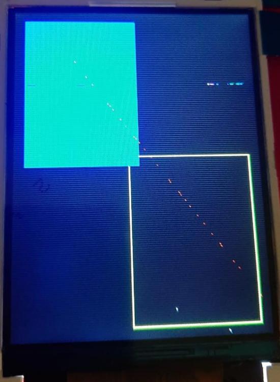
hai, before it i have done make data aquition with ADC external using SPI DMA...
but when i mix it in uGFX, interrupt not show up... anyone can help?
this is my code
-------------------------------------------------------------------------------------------------------------------------------------------------------------------
#if 1
//DMA1 stream 3
CH_FAST_IRQ_HANDLER(STM32_DMA1_CH3_HANDLER){
CH_IRQ_PROLOGUE();
chSysLockFromISR();
// THIS IS NEVER RUNNING
palSetLine(LINE_ARD_D4);
palClearLine(LINE_ARD_D4);
//TCIF[3:0]: stream x transfer complete interrupt flag (x = 3..0)
//in DMA low interrupt status register (DMA_LISR)
if ((DMA1->LISR & DMA_LISR_TCIF3) != 0) {
//NSS high
SPI2->CR1 |= SPI_CR1_SSI;
//disable SPI
SPI2->CR1 &= ~SPI_CR1_SPE;
stop_sclk();
palSetLine(LINE_ARD_D4);
uint32_t e_adc = (ADC_ConvertedValue[0] << 16) | (ADC_ConvertedValue[ 1 ]);// & 0xFF00);
if(titik_spi<SAMPLING_AMBIL){
#ifdef LIHAT_HEX
data_sample[titik_spi] = e_adc;
#else
data_sample[titik_spi] = e_adc & 0xffffff00;
#endif // DEBUG
titik_spi++;
}else sudah_penuh=true;
//CTCIF[3:0]: stream x clear transfer complete interrupt flag (x = 3..0)
//Writing 1 to this bit clears the corresponding TCIFx flag in the DMA_LISR register.
DMA1->LIFCR |= DMA_LIFCR_CTCIF3;
palClearLine(LINE_ARD_D4);
spi_process++;
}
chSysUnlockFromISR();
CH_IRQ_EPILOGUE();
}
#endif
// this is run in main function
void dma_config(){
// enable clock dma1
RCC->AHB1ENR |= RCC_AHB1ENR_DMA1EN;
// de init dma
DMA1_Stream3->CR = 0;
DMA1_Stream3->FCR = 0;
DMA1_Stream3->NDTR = 0;
DMA1_Stream3->PAR = 0;
DMA1_Stream3->M0AR = 0;
uint32_t tmpreg = 0;
/*------------------------- DMAy Streamx CR Configuration ------------------*/
/* Get the DMAy_Streamx CR value */
tmpreg = DMA1_Stream3->CR;
/* Clear CHSEL, MBURST, PBURST, PL, MSIZE, PSIZE, MINC, PINC, CIRC and DIR bits */
tmpreg &= ((uint32_t)~(DMA_SxCR_CHSEL | DMA_SxCR_MBURST | DMA_SxCR_PBURST | \
DMA_SxCR_PL | DMA_SxCR_MSIZE | DMA_SxCR_PSIZE | \
DMA_SxCR_MINC | DMA_SxCR_PINC | DMA_SxCR_CIRC | \
DMA_SxCR_DIR));
/* Configure DMAy Streamx: */
/* Set CHSEL bits according to DMA_CHSEL value */
tmpreg |= 0; //000: channel 0 selected
/* Set DIR bits according to DMA_DIR value */
tmpreg |= 0; //00: peripheral-to-memory
/* Set PINC bit according to DMA_PeripheralInc value */
tmpreg |= 0; //0: peripheral address pointer is fixed
/* Set MINC bit according to DMA_MemoryInc value */
tmpreg |= DMA_SxCR_MINC; //1: memory address pointer is incremented after each data transfer (increment is done according to MSIZE)
/* Set PSIZE bits according to DMA_PeripheralDataSize value */
tmpreg |= DMA_SxCR_PSIZE_0; //01: half-word (16-bit) (8 bit)
/* Set MSIZE bits according to DMA_MemoryDataSize value */
tmpreg |= DMA_SxCR_MSIZE_0; //01: half-word (16-bit)
/* Set CIRC bit according to DMA_Mode value */
tmpreg |= 0; //0: circular mode disabled
/* Set PL bits according to DMA_Priority value */
tmpreg |= DMA_SxCR_PL_1 | DMA_SxCR_PL_0; //11: very high
/* Set MBURST bits according to DMA_MemoryBurst value */
tmpreg |= 0; //00: single transfer
/* Set PBURST bits according to DMA_PeripheralBurst value */
tmpreg |= 0; //00: single transfer
/* Write to DMAy Streamx CR register */
DMA1_Stream3->CR = tmpreg;
/*------------------------- DMAy Streamx FCR Configuration -----------------*/
/* Get the DMAy_Streamx FCR value */
tmpreg = DMA1_Stream3->FCR;
/* Clear DMDIS and FTH bits */
tmpreg &= (uint32_t)~(DMA_SxFCR_DMDIS | DMA_SxFCR_FTH);
/* Configure DMAy Streamx FIFO:
Set DMDIS bits according to DMA_FIFOMode value
Set FTH bits according to DMA_FIFOThreshold value */
//WE NOT USE FIFO!!!!
tmpreg |= DMA_SxFCR_FTH_0; //01: 1/2 full FIFO
/* Write to DMAy Streamx CR */
DMA1_Stream3->FCR = tmpreg;
/*------------------------- DMAy Streamx NDTR Configuration ----------------*/
/* Write to DMAy Streamx NDTR register */
DMA1_Stream3->NDTR = 2; // 16 bit * 2
/*------------------------- DMAy Streamx PAR Configuration -----------------*/
/* Write to DMAy Streamx PAR */
//dari OVM
#define SPI3_DR_ADDRESS ((uint32_t) 0x40003C0C) /* lihat halaman 709 dan table 1 hal 50 */
#define SPI2_DR_ADDRESS ((uint32_t) 0x4000380C)
DMA1_Stream3->PAR = (uint32_t)SPI2_DR_ADDRESS;
/*------------------------- DMAy Streamx M0AR Configuration ----------------*/
/* Write to DMAy Streamx M0AR */
DMA1_Stream3->M0AR = &ADC_ConvertedValue[0];
// /* Enable the selected DMA transfer interrupts */
DMA1_Stream3->CR |= DMA_SxCR_TCIE; //| DMA_SxCR_HTIE | DMA_SxCR_TEIE | DMA_SxCR_DMEIE;
//STM32_GPT_TIM5_IRQ_PRIORITY
//STM32_SPI_SPI2_DMA_PRIORITY
nvicEnableVector(DMA1_Stream3_IRQn,2);//CORTEX_PRIO_MASK
tmpreg = DMA1_Stream3->CR;
chprintf(chp,"---> See DMA1_Stream3->CR = 0x%x\r\n",tmpreg);
tmpreg = DMA1_Stream3->FCR;
chprintf(chp,"---> See DMA1_Stream3->FCR = 0x%x\r\n",tmpreg);
tmpreg = DMA1_Stream3->NDTR;
chprintf(chp,"---> See DMA1_Stream3->NDTR = 0x%x\r\n",tmpreg);
tmpreg = DMA1_Stream3->PAR;
chprintf(chp,"---> See DMA1_Stream3->PAR = 0x%x\r\n",tmpreg);
tmpreg = DMA1_Stream3->M0AR;
chprintf(chp,"---> See DMA1_Stream3->MOAR = 0x%x\r\n",tmpreg);
}
thank u...